Balancing Robot

Over a year ago I started to work on a small balancing robot. Between learning more about communication protocols and feedback loops I also had periods of schoolwork that kept me from this hobby. In the end my little robot was balancing on his own and I could send steering and throttle commands wirelessly.

This project marked many firsts for me. It was the first time I made use of my microcontroller's I2C, UART and ADC peripherals. It was the first time I heard about PID control loops. It was also the first time I used an RF module to communicate wirelessly.

As I progressed I took several photos and video clips when milestones were met.

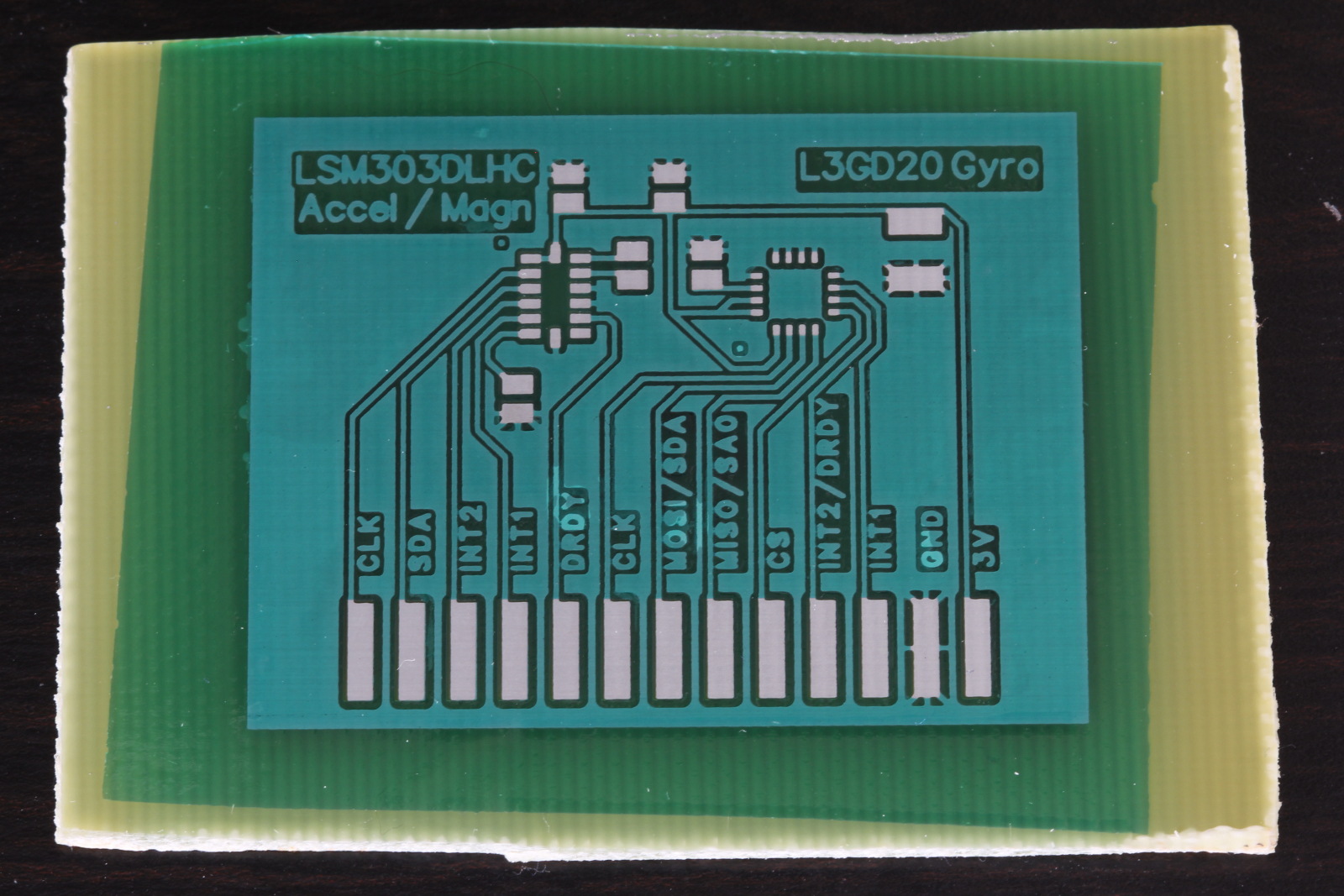
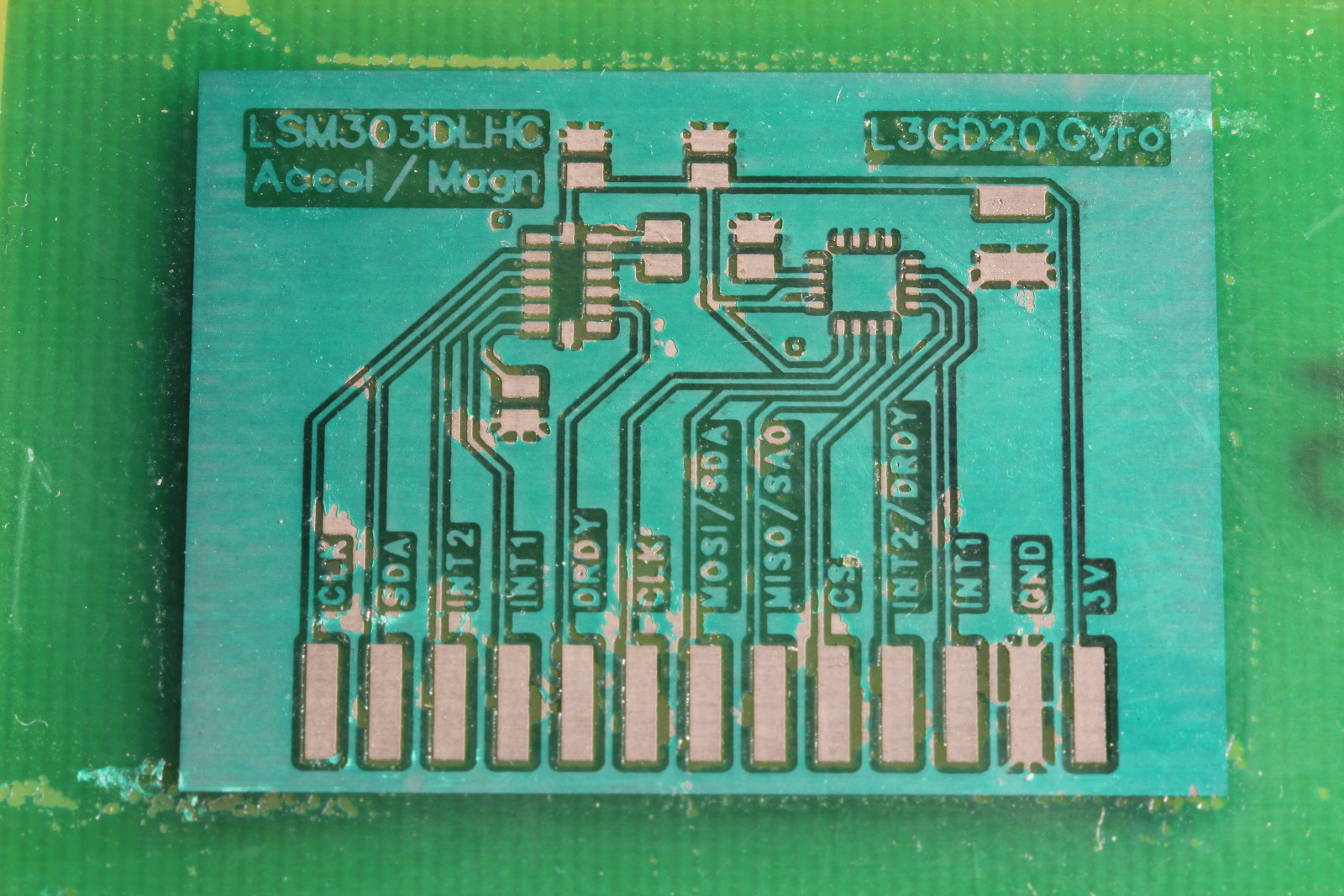
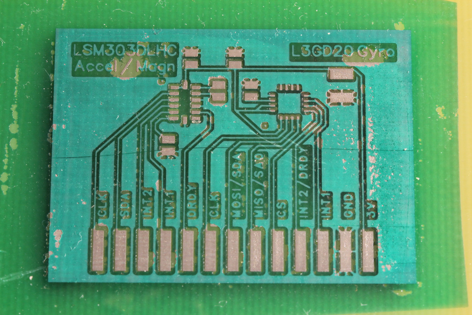
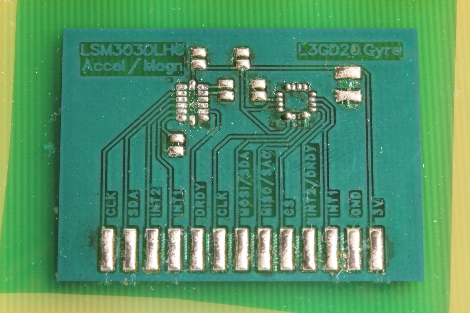
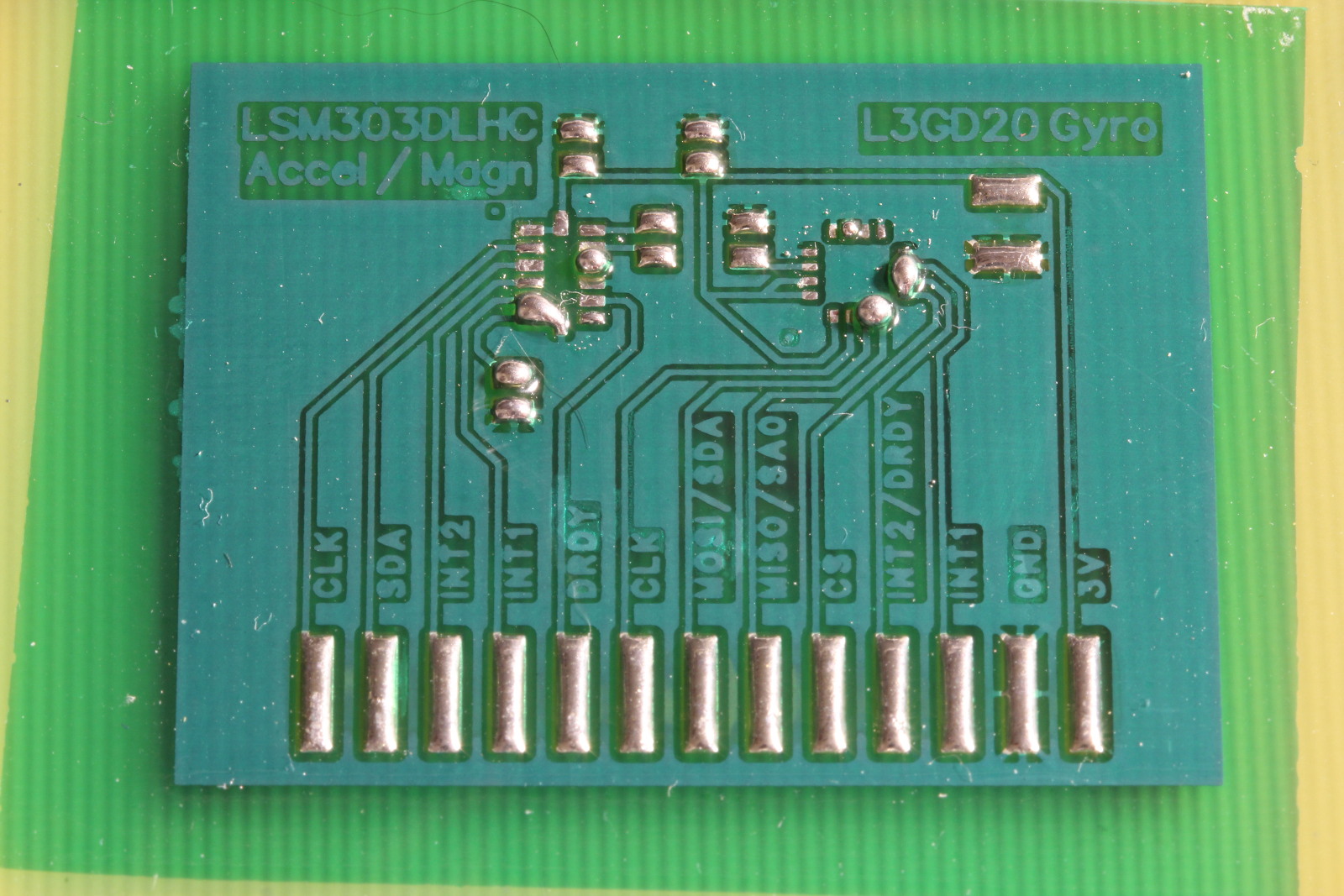
During the planning stage I selected a 3-axis gyro and a 3-axis accelerometer. I settled on STM's L3GD20 and LSM303DLHC devices. I laid out and etched a breakout board for them, then wrote a little Hello World test to draw bar graphs for the gyro readouts.

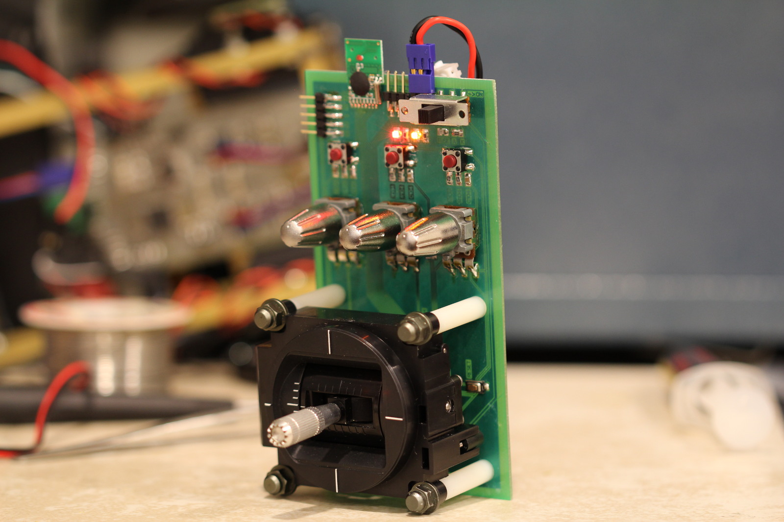
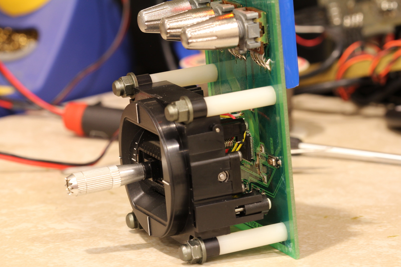
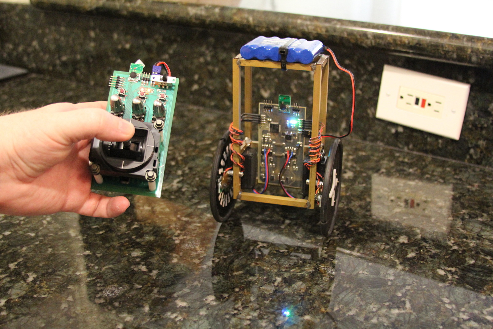
I decided to use a pair of RC hobby servos to power the robot. I removed the feedback potentiometers and modified the output gears to allow for continuous rotation. Some steering wheels from RC hobby transmitters were initially used as the wheels. The robot frame was constructed with some brass square tubing cut to length and soldered together. A gimbal was used for steering and throttle inputs since I didn't want to dive into the 2.4GHz module's lengthy datasheet until the end.

The wheels quickly proved to be a problem. While they had great traction, their diameter was far too small. The robot could easily drift a little too much, and the servos at full power couldn't spin fast enough to overcome the drifting.

I went with larger diameter wheels, making it much easier for the robot to balance:

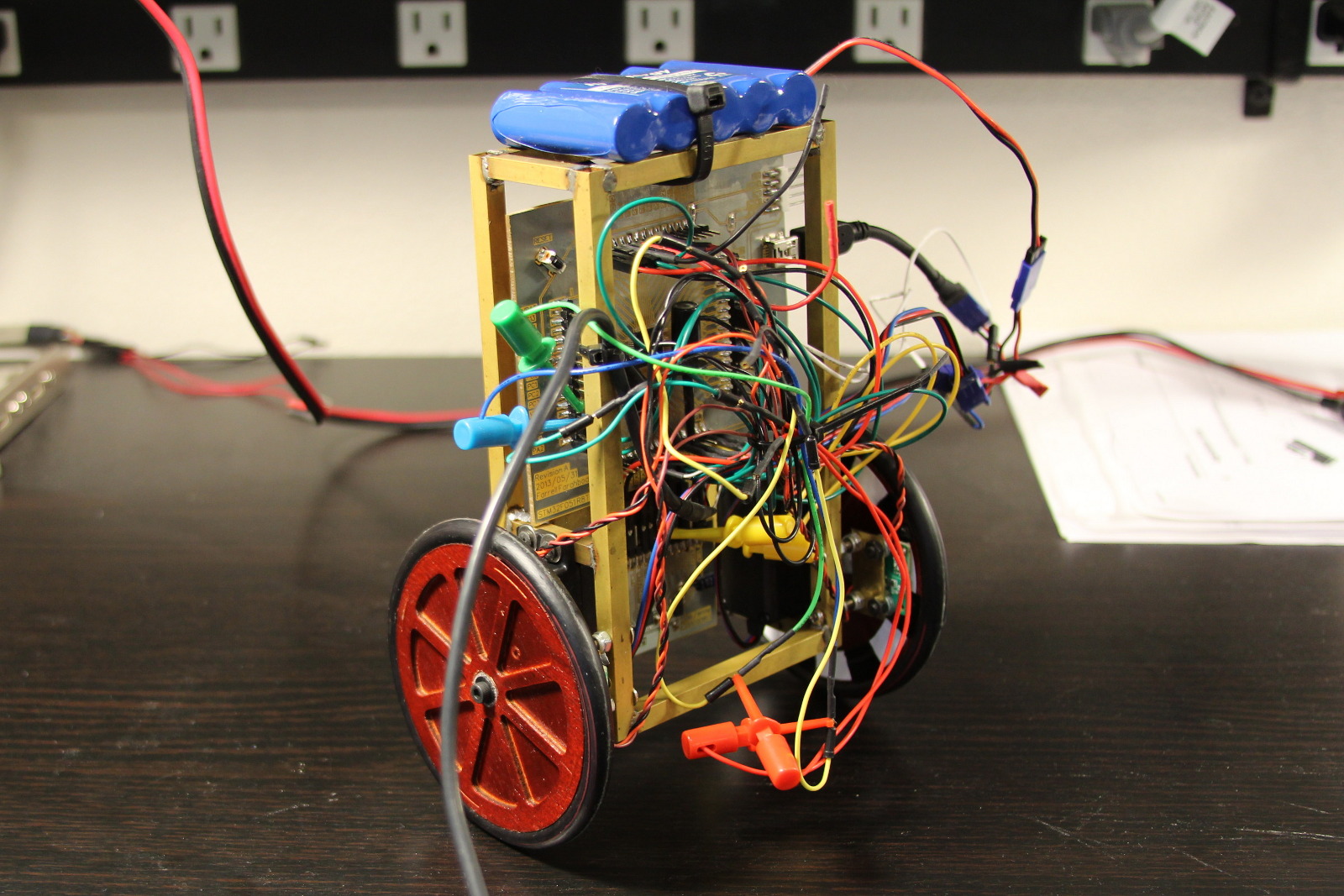
The robot was actually drivable at this point. I added optical wheel encoders to make it easier to sense when the robot started to drift off course. Without the encoders the robot could drift if the driving surface wasn't perfectly level. By now the little guy was a mess of breakout boards, flying wires and extensions.

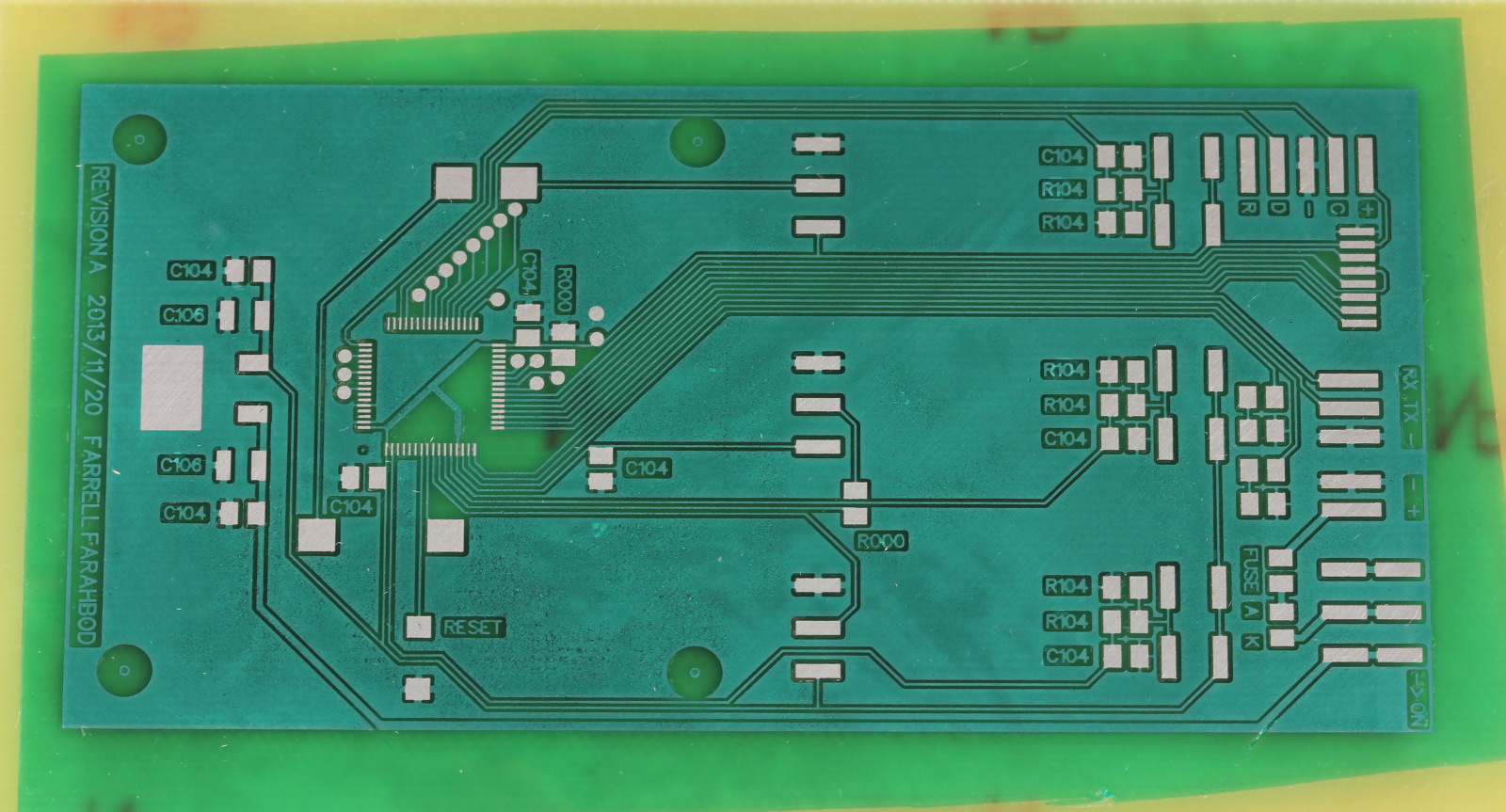
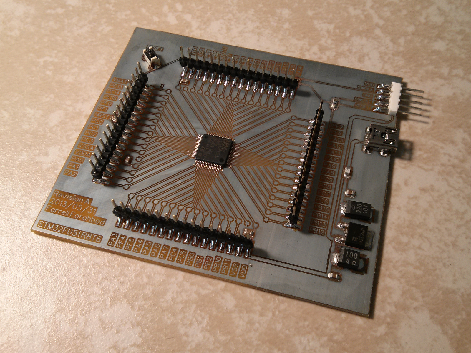
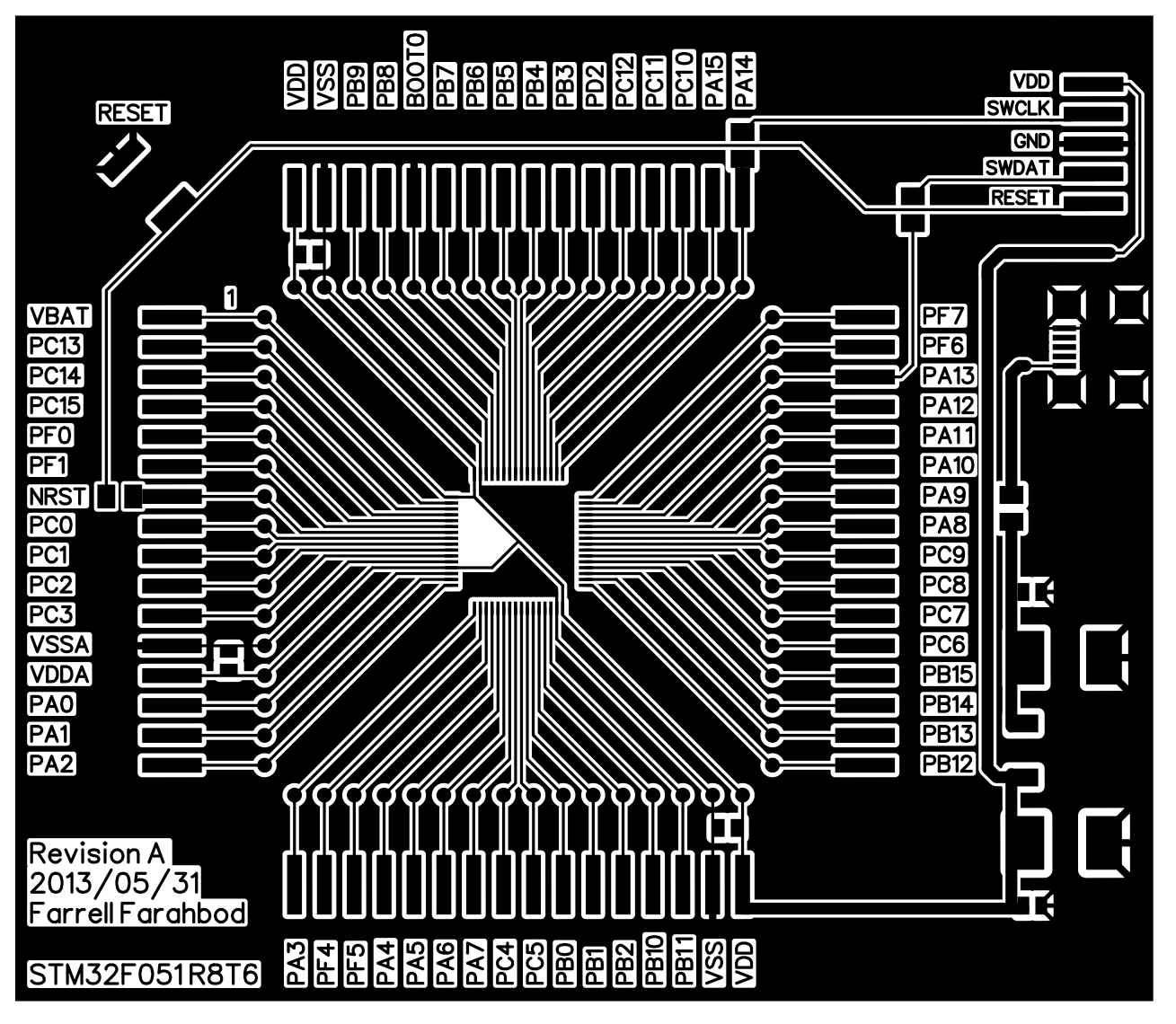
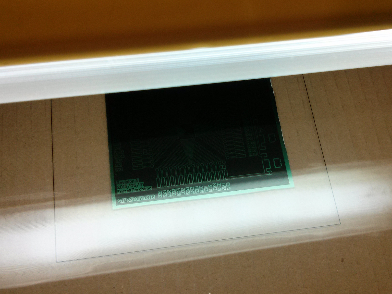
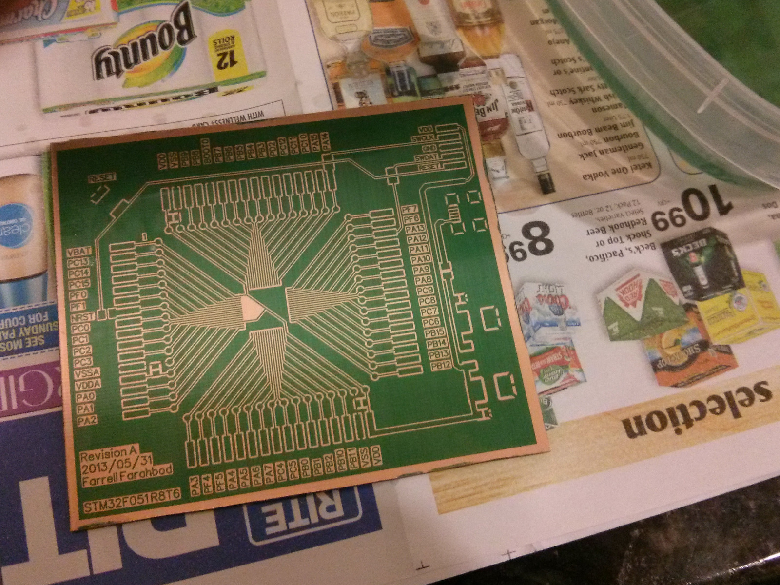
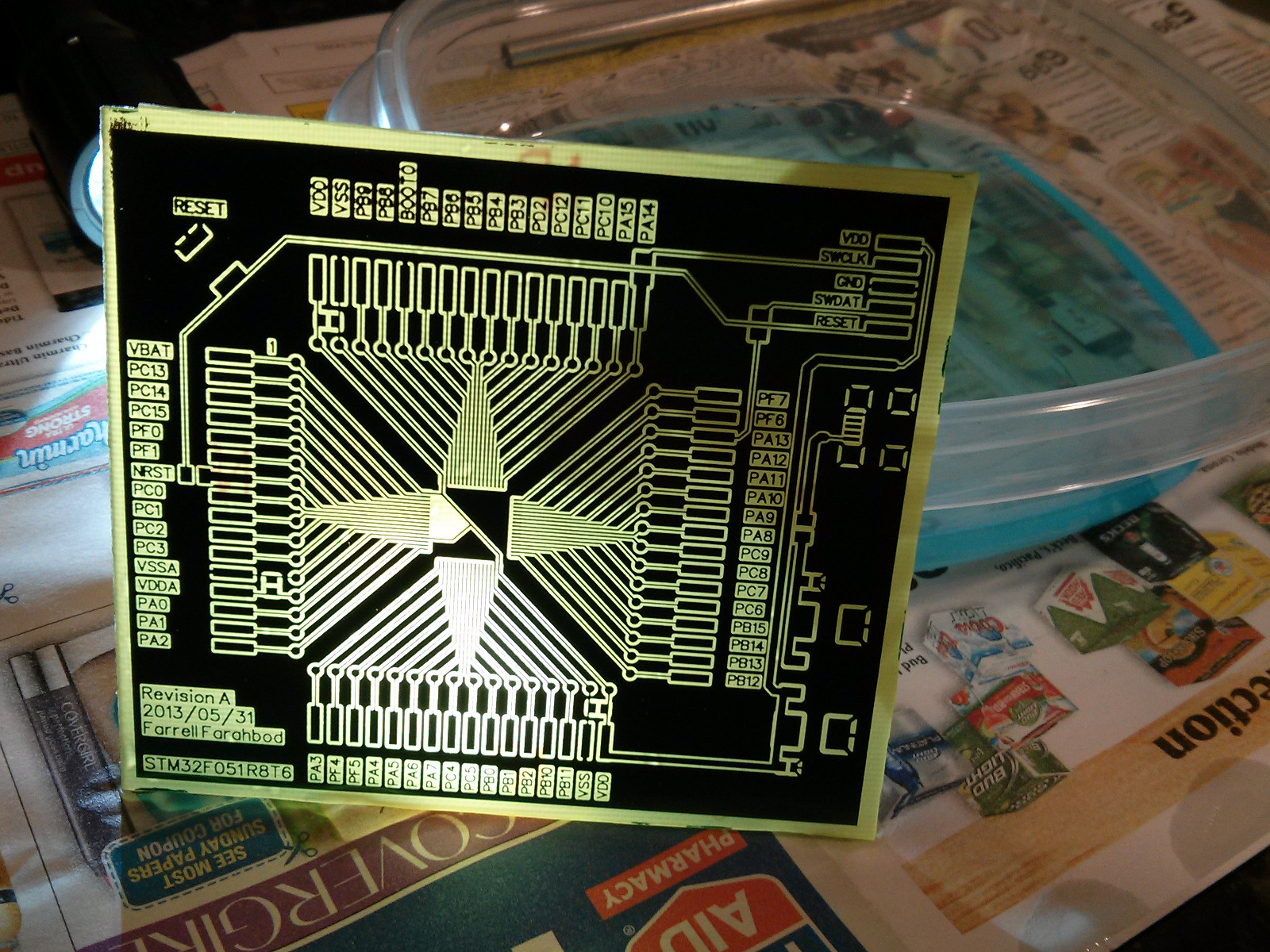
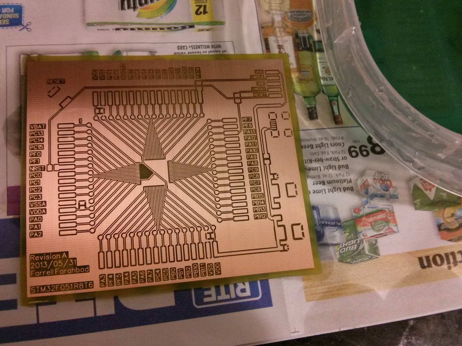
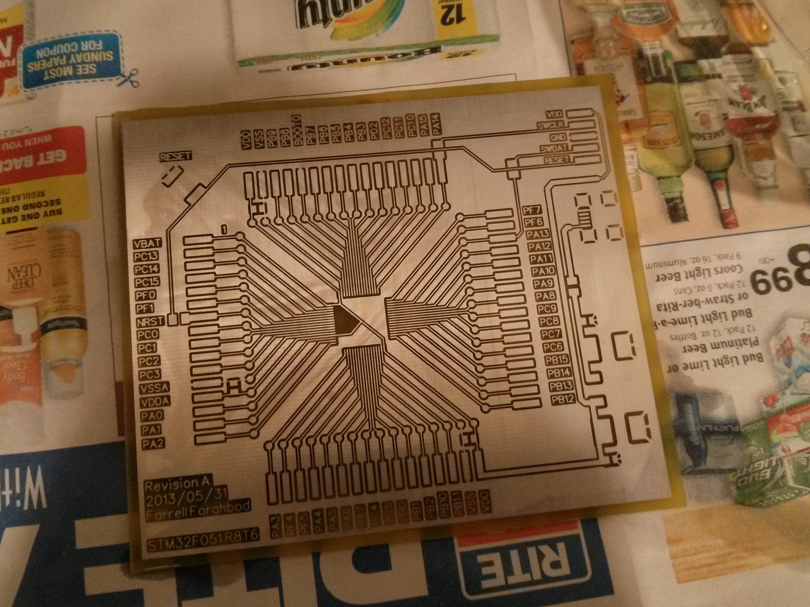
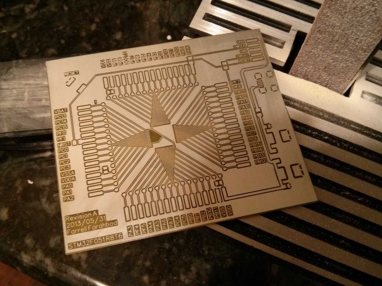
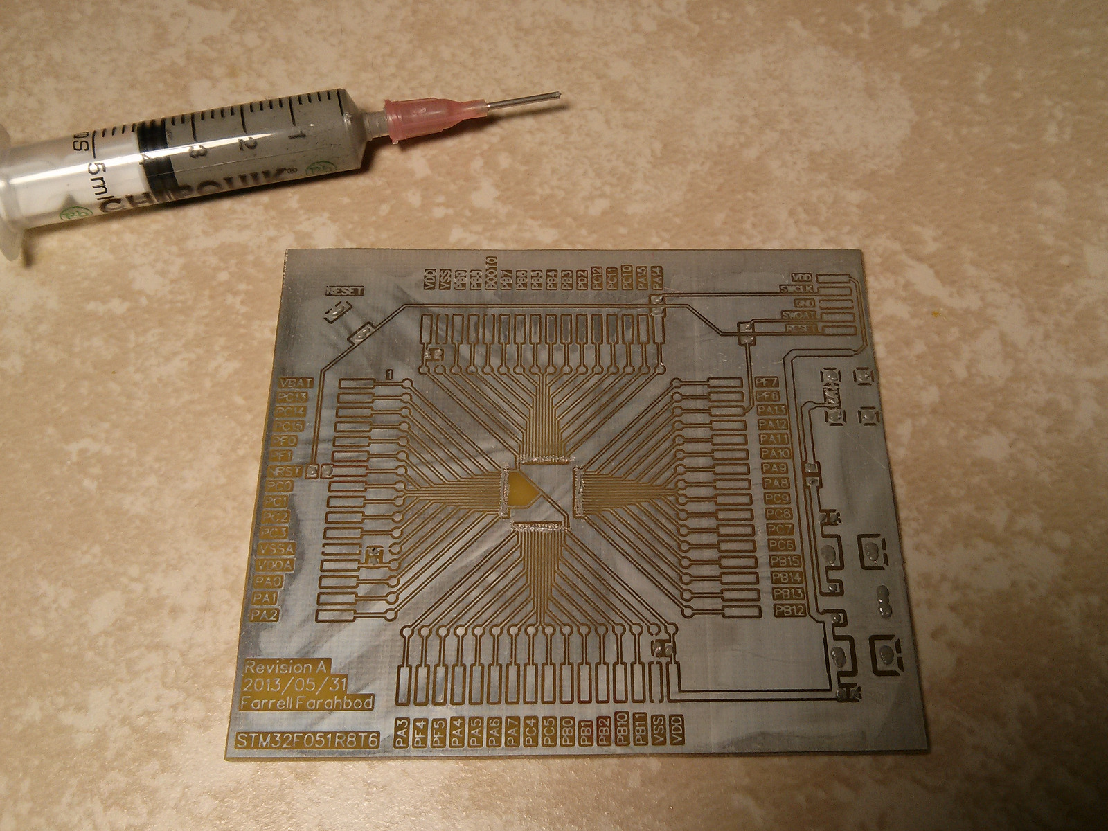
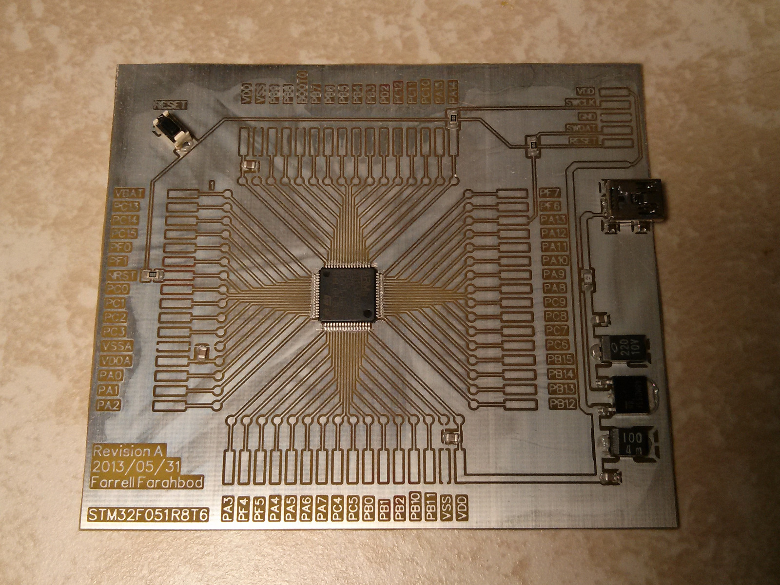
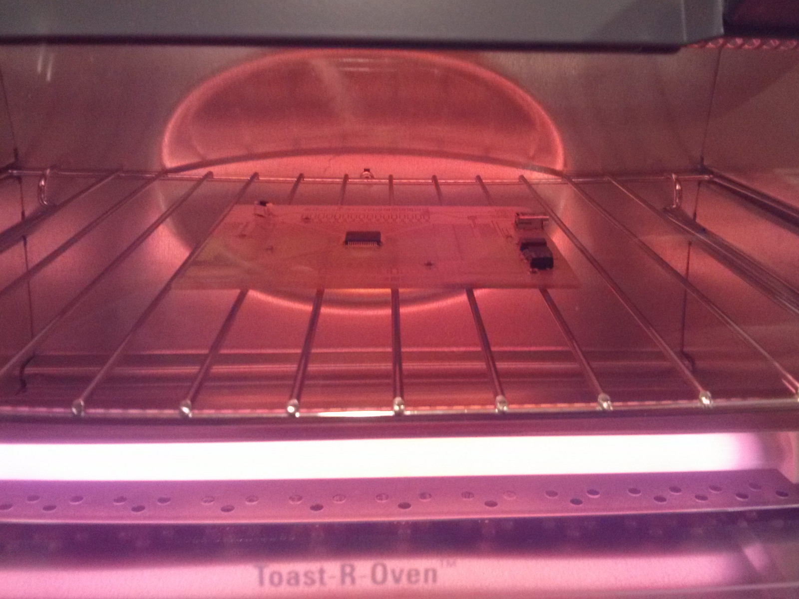
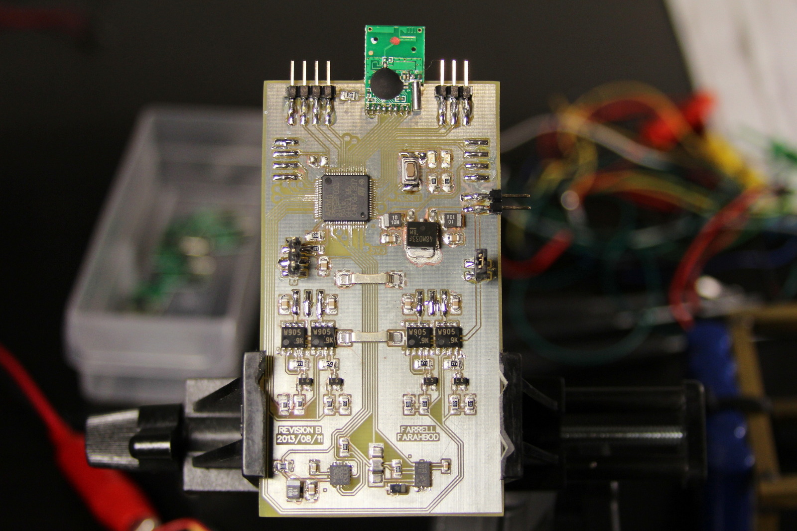
To clean up the mess I designed and etched a PCB specifically for this robot. I incorporated dual H-Bridges on the PCB to give better control over the motors. Previously I had just generated servo signals and let the servos' PCBs control the motors. This mostly worked, but as the servo PCBs came up to temperature the signal center point would drift slightly. This meant that after about a minute of use the robot would effectively have a bit of steering and throttle applied.

I finished by designing and etching a PCB for the transmitter. That was shown in my earlier post about solder masks. A little tuning of the PID control loop brought everything together and I was done. I'll post the firmware in a few days after doing the last bits of clean up and documentation.

DIY PCBs with Solder Mask

I’ve managed to get decent solder masks on my home made PCBs. The dry film variety has worked best for me, with liquid masks being difficult to apply consistently. To perfect my process I used a small gyro / accelerometer / magnetometer breakout PCB that I designed around a year ago. Here’s the end result:

It’s not perfect — there are some spots with delamination — but the result is usable and very functional. It works just like the professional stuff. It tolerates abuse from an iron at 375C without damage. It sticks well and doesn’t scratch easily.

It took about eight failures, due to various problems, before I got to this point. I’m using Dynamask 5000 Dry Film Solder Mask. It’s sold in giant rolls, but small amounts can be purchased through eBay (search for “dry film solder mask”) for about $7 per square foot.

My process:

  1. Etch and tin plate the PCB (per my earlier blog post, but don’t sand the PCB to it’s final shape until after the solder mask is done.)
  2. Cut a piece of solder mask to size. It should be big enough to cover all of the copper, but not hang out past the edge of the PCB. If it hangs out, it can gum up the laminator.
  3. Make a 10% alcohol solution in water. I used SLX Denatured Alcohol from a local hardware store. Wet the entire surface of your PCB with it, using a q-tip. Don’t flood the board, but there needs to be a film over everything. This helps prevent air bubbles when you laminate.
  4. Peel the protective film off of the solder mask, place it on the PCB, and press the leading edge onto the PCB so it won’t slip around. Run it through the laminator at a low temperature two or three times.
  5. Let it sit for 30 minutes.
  6. Expose. With my UV lamp from MG Chemicals, this takes 10 minutes.
  7. Let it sit for 30 minutes.
  8. Remove the other protective film.
  9. Develop with half a gram of sodium carbonate per 12oz of water. It takes about five minutes to develop. Gently brush to remove the unexposed mask.
  10. Expose for 30 minutes.
  11. Bake at 145C for 30 minutes.

As I mentioned earlier, it took many attempts before I got a useable mask. Here are the problems I encountered:

Bubbles under the mask. If you follow the datasheet you’re supposed to use a vacuum laminator, but that’s outside the realm of a hobbyist. Little pockets of air will get trapped when using a hot roll laminator or an iron. I first tried using water to prevent air pockets, but it didn’t help much. Adding a bit of alcohol helped, perhaps the alcohol slightly “melts” into the uncured solder mask. Bubbles still occur, but there are fewer of them and they don’t usually break when you develop the mask. Without the alcohol your bubbles will break and yield an ugly surface:

Blotchy or satin sheen on the mask. This happens when the developer is too strong. I found 1 gram of sodium carbonate per 12oz of water to be too strong, and half a gram to be just right. This might change based on temperature — my stuff was all at around 70F.

Don’t forget to bake the board at the end. The final cure requires both UV exposure and the baking process, otherwise the mask will not fully harden. Even if you will use solder paste and reflow the board, you should still bake the board before doing that. You can easily gouge the mask while placing parts with tweezers.

I noticed that the flux in Chipquik’s SMD291SNL lead-free paste (Sn 96.5 / 3 Ag / 0.5 Cu) was very aggressive and would creep under the solder mask. Even without a solder mask, their flux will do a little damage to tinned copper. I have not had any problems with other solder pastes and I currently use Kester EP256 leaded paste.

Chipquik paste:

Kester paste:

After getting the process figured out I decided to make a simple 2.4GHz transmitter for use with my robots. The PCB is below. The ugly looking ground fill is due to an overexposed photomask which allowed the etchant to slightly damage the surface.

It turned out well. Imperfections only appear if you look up close.

I think the finished project turned out very well.

Working with the HC-06 Bluetooth Serial Module

I recently got a BT2S Bluetooth Serial adapter. It's easy to use and the range is good when you consider that bluetooth is intentionally short range. I can have the BT2S about 40 feet away, with three walls between it and my computer, and still get good performance. The BT2S is an HC-06 Slave Mode module mounted on a breakout board with an LED and some other SMDs.

The bluetooth adapters can be purchased for around $7 from China or around $10 locally.

My adapter came with no documentation, so here are my notes:

1. I powered the module with 3V, but most web sites claim it can handle up to 5V.

2a. The default configuration is 9600 8N1, device name = HC-06, PIN = 1234. If you don't want to change any of this you can skip the configuration steps and use the device as-is.

2b. Changing the configuration requires a USB Serial ("an FTDI") adapter. As usual, cross the TX/RX lines. Configuration must be done when the BT2S is NOT paired with a bluetooth device.

2c. In Linux, connect to the FTDI with $ screen /dev/ttyUSB0 9600

2d. Commands are simple ASCII text, with no need for a newline or carriage return. Each complete command must be entered in less than one second, so type them out in a text editor, then paste them into screen. The command will not be echoed back, but a response will be sent.

2e. There are a handful of commands to set the device name, PIN, baud rate and parity. Settings are stored in non-volatile memory. Erich Styger has a nice table of the commands and responses on his blog: http://mcuoneclipse.com/2013/06/19/using-the-hc-06-bluetooth-module/

3. Using the device is straight forward. Connect the TX and RX lines as needed, then power it up. The red LED blinks when not paired, and will be solid red when paired and in use. Pair the device, then use screen (or cat or whatever) and treat it like a regular serial device. There is no need to specify the baud rate as that seems to be handled by the bluetooth drivers.

In Linux the device will be /dev/rfcomm0, and in Mac OS the device will be /dev/tty.DeviceName-DevB (where DeviceName is the bluetooth device name, "HC-06" by default)

I noticed that the BT2S paired perfectly with the built-in bluetooth of my MBP, but with Linux in a VM it would pair but fail to make the /dev/rfcomm0 device. Using a bluetooth dongle had the same effect. I was able to get it working by doing the following:

1. Determine the bluetooth device id with $ sudo hcitool scan

2. Create the /dev/rfcomm0 device with $ sudo rfcomm bind /dev/rfcomm0 20:13:11:05:12:02 1
(replace 20:13:11:05:12:02 with your device ID if it's different)

3. Optionally change permissions with $ sudo chmod 777 /dev/rfcomm0

The BT2S also works with my Nexus 4 phone. I've tried a few different bluetooth terminal apps, and they all pair and work fine. I've noticed that at 9600 baud everything works perfectly, but at 115200 baud the apps get very slow and errors occur about once per second. I'm not sure if the problem is with the apps, the Android bluetooth stack, or the phone itself. Regardless, the 115200 baud rate works fine with Linux and Mac OS.

Overclocking the TI-83+ Graphing Calculator

My biggest gripe with the TI-83+ is its slow performance — it becomes painful when using this graphing calculator to actually graph stuff. There are many web sites that cover how to overclock this calculator, but unfortunately they all detail the procedure for revision F of the PCB. I have a calculator from around 2000 or 2001, and it's PCB revision A. I did some poking around near the main IC, and managed to figure it out.

Here's a short clip showing the end result. First, three sine waves are graphed at the stock clock rate. Then I flip a switch, and graph the same sine waves again, but at nearly double the speed.

An RC oscillator is used for the clock, so if you just reduce the capacitance you can speed up the clock. You can either replace the capacitor, or better yet, wire a second capacitor in series. By wiring a second capacitor in series you can use a switch to short out the new capacitor and return the clock to its original speed. This is helpful for two reasons: overclocking drains the batteries quicker, and playing games can get difficult when they run at almost double speed. The TI-83+ case doesn't leave much room, but there is just enough space for a small switch to be added in the battery compartment.

I probed all of the passives near the main IC, looking for any waveforms with a relatively high frequency. After a couple minutes I found the right capacitor and began wiring various capacitors in series. My particular calculator runs stable at up to about 10.2MHz. I can push it further, but the LCD starts to glitch. Pixels that should be black are not, and others that should be white are actually black. At about 13.5MHz my calculator's LCD would no longer work at all. Here's a list of the caps I tried in series with the stock cap, and the resulting clock rates I measured:

Stock clock = 5.5MHz
82pF resulted in 6.8MHz (stable)
27pF resulted in 8.7MHz (stable)
12pF resulted in 9.4MHz (stable)
10pF resulted in 10.2MHz (stable)
7pF resulted in 11.3MHz (LCD glitches)
4pF resulted in 13.5MHz (LCD will not work)

The clock rate is measured by probing the right side of the resistor located directly above the capacitor that is standing on end.

Here's the waveforms, stock and overclocked:

I hope this helps someone else with an old revision of the TI-83+.

PCB Design and Etching

I recently designed a breakout board for the STM32F0. The official STM board is great (and cheap) but I wanted a single-sided board. My laptop has a metal case, and it's tempting to rest a PCB on it sometimes. I'd hate to short out the pin headers.

The end result:

The board is simple: an F0, pin headers for every pin, test points for every pin, a reset button, and a USB port with an LDO regulator to provide 3.3V. I couldn't find surface mount headers locally, so I made some through-hole ones work.

Step 1: Layout the PCB with gEDA.


Step 2: Print the design to a transparency, cut a board to size, and expose it with a UV lamp.


Step 3: Develop the board, then rinse it off.


Step 4: Etch the board. I used sodium persulfate for this project.


Step 5: Remove the remaining mask by placing the board back into the developer.


Step 6: Tin plate the board.


Step 7: Sand the board to clean up the edges.


Step 8: Apply solder paste for the SMDs.


Step 9: Place the SMDs.


Step 10: Bake until the solder melts.


Step 11: Hand-solder the pin headers, then clean the board with some flux remover.


Now I have a board that can be placed on an electrically-conductive surface without fear. I think the four-way layout of pin headers will also make it easier to transition from a prototype to a custom PCB layout.

< Prev  2  Next >